![]()
![]()
![]()
![]()
![]()
![]()
![]()
![]()
![]()
![]()
![]()
|
|
|
|
VP7206 Technical Information
Description of Operation This amplifier combines switching and linear circuitry to gain additional power with small size. The high voltage output is proportional to the signal input with direct coupling and wide bandwidth. The output is equally capable of sourcing and sinking current to drive capacitive loads. With reference to the block diagram below, the input signal is first preamplified and the signal output of the preamplifier drives the switch mode step up controller which, in conjunction with the step up transformer, provides a high voltage output proportional to the signal input. Before this DC output is applied to the output filter, the linear step down controller provides sinking current to the output as necessary. The crossover controller smoothes the output between the step up and step down controllers. Current limiting is included for output overload protection and the bias voltage generator provides ±12V internal power following the DC input power filter.
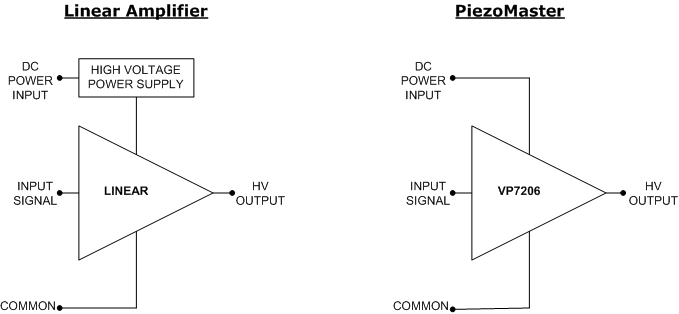
Efficiency Comparison The overall efficiency of the VP7206 amplifier series is approximately twice as good as a linear amplifier. Shown below is a typical linear amplifier with an external high voltage power supply compared with the PiezoMaster amplifier that does not require a high voltage power supply. Since the PiezoMaster amplifier steps up the output voltage to precisely that voltage demanded by the signal input, there is no need for a high voltage power supply and no corresponding loss of efficiency.
Because the high voltage power supply is generally selected with a voltage 10% higher than the maximum required output voltage of the linear amplifier, the resulting efficiency of the linear amplifier is typically 45%. With a 75% efficiency for the high voltage power supply, the resulting overall efficiency for the combination is 34% versus 70% for the PiezoMaster. For an application that varies below 50% of its maximum output voltage, the improvement in efficiency is even more significant.
Mounting and Cooling With the small size of this amplifier, it can be mounted close to the high voltage load which limits access to hazardous wiring. The various connector and cover options allow mounting to the internal or external surface of an enclosure or directly to a PC board. Refer to the outline drawings below for dimensions and mounting screw requirements. The mounting surface of the amplifier is the heat sink for the internal components. For many applications, this heat sink is sufficient to maintain the amplifier temperature below the level that will initiate the internal thermal protection. For some applications, additional heat sinking or forced air cooling will be needed. For additional heat sinking, the amplifier can be mounted to a larger metal surface or supplementary heat sinks can be attached.
Outline drawing of open frame with top access connectors.pdf This version is intended to be mounted within an enclosure with all three connectors accessible from the top.
Outline drawing of fully enclosed with end access connectors.pdf This version is intended to be mounted within an enclosure with access to the J1 and J4 connectors. Otherwise, this unit is fully covered. The J5 connector option is not available with this version.
Outline drawing of fully enclosed with bottom access connectors.pdf This version is intended to be mounted externally to an enclosure with access to all three connectors through the bottom of the unit and through the enclosure wall. Note that the J4 connector pins are reassigned for this version only.
Outline drawing of fully enclosed with PC mounting.pdf This version is intended to be directly mounted onto a PC board with the connectors directly soldered to the PC board. The unit can be mounted against the board or raised above the board to save space for other small components.
Wiring and Connections To use the PiezoMaster amplifier, it must be connected to an input signal source, a DC power source and an output piezo stack. For best operation , the DC power source should be isolated from the signal source with both signal and power source having a separate return connection as shown by the wiring diagram #1. This is best because the signal source wiring does not share any of the power supply noise which is reduced by a common mode filter within the VP 7206 amplifier.
If the signal source and the power source share the same common due to a non-isolated system power supply, then the connections should be made per wiring diagram #2 . A single wire should be used for the common return to avoid a ground loop. Also, the connection at the VP7206 between power minus and common should be short.
With a slight change in connections to the stack as shown by wiring diagram #3, the VP7206 amplifier will shift the output voltage range negatively by the voltage of the DC power source. This will allow the amplifier to apply a small negative voltage (up to the DC power supply voltage limit) to the piezo stack. As an example, if the range is 400V and the bias is 50% and the piezo stack return is connected to common, then with 0 VDC input signal, the output will be at +200VDC with a range of 0 VDC to +400 VDC. If the piezo stack return is reconnected to the power pin and the DC input power supply is 50 VDC, then with 0 VDC input signal, the output will be at +150 VDC with a range of -50 VDC to +350 VDC.
The chassis ground is an important connection for safety and noise performance. This connection can best be made to a central chassis ground point. If a chassis ground connection is not available, then this pin should be connected to the common return for the DC input power source.
|
|
Low Price Efficient Requires No Power Supply Fully Customizable Ultra Small Size |